- 您现在的位置:买卖IC网 > Sheet目录3871 > PIC18F4682T-I/ML (Microchip Technology)IC PIC MCU FLASH 40KX16 44QFN
2011 Microchip Technology Inc.
DS39931D-page 125
PIC18F46J50 FAMILY
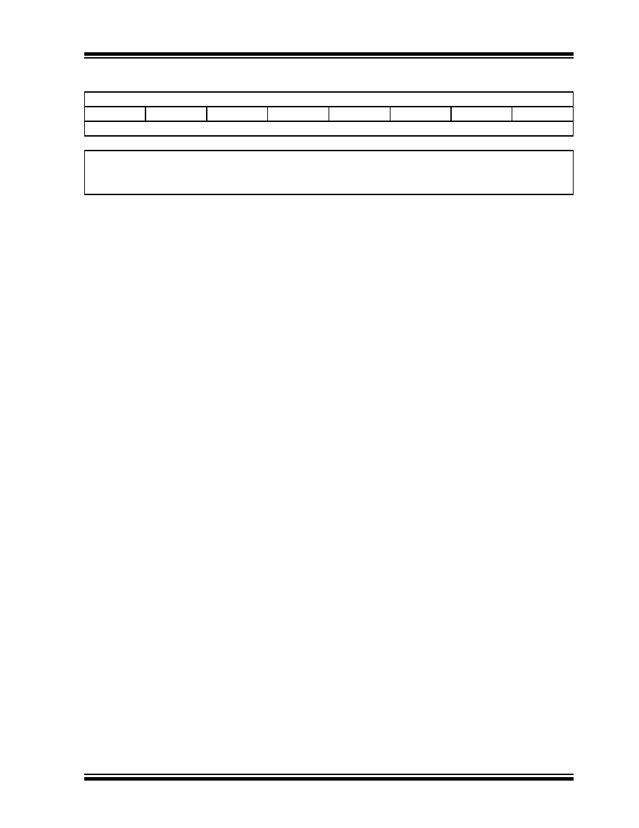
REGISTER 9-9:
PIE3: PERIPHERAL INTERRUPT ENABLE REGISTER 3 (ACCESS FA3h)
R/W-0
SSP2IE
BCL2IE
RC2IE
TX2IE
TMR4IE
CTMUIE
TMR3GIE
RTCCIE
bit 7
bit 0
Legend:
R = Readable bit
W = Writable bit
U = Unimplemented bit, read as ‘0’
-n = Value at POR
‘1’ = Bit is set
‘0’ = Bit is cleared
x = Bit is unknown
bit 7
SSP2IE:
Master Synchronous Serial Port 2 Interrupt Enable bit
1
= Enabled
0
= Disabled
bit 6
BCL2IE:
Bus Collision Interrupt Enable bit (MSSP2 module)
1
= Enabled
0
= Disabled
bit 5
RC2IE:
EUSART2 Receive Interrupt Enable bit
1
= Enabled
0
= Disabled
bit 4
TX2IE:
EUSART2 Transmit Interrupt Enable bit
1
= Enabled
0
= Disabled
bit 3
TMR4IE:
TMR4 to PR4 Match Interrupt Enable bit
1
= Enabled
0
= Disabled
bit 2
CTMUIE:
Charge Time Measurement Unit (CTMU) Interrupt Enable bit
1
= Enabled
0
= Disabled
bit 1
TMR3GIE
: Timer3 Gate Interrupt Enable bit
1
= Enabled
0
= Disabled
bit 0
RTCCIE
: RTCC Interrupt Enable bit
1
= Enabled
0
= Disabled
发布紧急采购,3分钟左右您将得到回复。
相关PDF资料
PIC24HJ128GP306T-I/PT
IC PIC MCU FLASH 128KB 64TQFP
PIC24FJ96GA008T-I/PT
IC PIC MCU FLASH 96KB 80TQFP
PIC24FJ64GA010T-I/PT
IC PIC MCU FLASH 64KB 100TQFP
PIC24FJ64GA008T-I/PT
IC PIC MCU FLASH 64KB 80TQFP
PIC18LF4450T-I/PT
IC PIC MCU FLASH 8KX16 44TQFP
PIC18LF2450T-I/ML
IC PIC MCU FLASH 8KX16 28QFN
PIC16F1937-I/ML
IC PIC MCU FLASH 512KX14 44-QFN
PIC18F25K20-E/ML
IC PIC MCU FLASH 16KX16 28-QFN
相关代理商/技术参数
PIC18F4682T-I/PT
功能描述:8位微控制器 -MCU 80KB FL 3328bytes RAM 36I/O RoHS:否 制造商:Silicon Labs 核心:8051 处理器系列:C8051F39x 数据总线宽度:8 bit 最大时钟频率:50 MHz 程序存储器大小:16 KB 数据 RAM 大小:1 KB 片上 ADC:Yes 工作电源电压:1.8 V to 3.6 V 工作温度范围:- 40 C to + 105 C 封装 / 箱体:QFN-20 安装风格:SMD/SMT
PIC18F4685-E/ML
功能描述:8位微控制器 -MCU 96KB 3328 RAM w/ECAN RoHS:否 制造商:Silicon Labs 核心:8051 处理器系列:C8051F39x 数据总线宽度:8 bit 最大时钟频率:50 MHz 程序存储器大小:16 KB 数据 RAM 大小:1 KB 片上 ADC:Yes 工作电源电压:1.8 V to 3.6 V 工作温度范围:- 40 C to + 105 C 封装 / 箱体:QFN-20 安装风格:SMD/SMT
PIC18F4685-E/P
功能描述:8位微控制器 -MCU 96KB 3328 RAM w/ECAN RoHS:否 制造商:Silicon Labs 核心:8051 处理器系列:C8051F39x 数据总线宽度:8 bit 最大时钟频率:50 MHz 程序存储器大小:16 KB 数据 RAM 大小:1 KB 片上 ADC:Yes 工作电源电压:1.8 V to 3.6 V 工作温度范围:- 40 C to + 105 C 封装 / 箱体:QFN-20 安装风格:SMD/SMT
PIC18F4685-E/PT
功能描述:8位微控制器 -MCU 96KB FL 3328bytes RAM 36I/O RoHS:否 制造商:Silicon Labs 核心:8051 处理器系列:C8051F39x 数据总线宽度:8 bit 最大时钟频率:50 MHz 程序存储器大小:16 KB 数据 RAM 大小:1 KB 片上 ADC:Yes 工作电源电压:1.8 V to 3.6 V 工作温度范围:- 40 C to + 105 C 封装 / 箱体:QFN-20 安装风格:SMD/SMT
PIC18F4685-I/ML
功能描述:8位微控制器 -MCU 96KB 3328 RAM w/ECAN RoHS:否 制造商:Silicon Labs 核心:8051 处理器系列:C8051F39x 数据总线宽度:8 bit 最大时钟频率:50 MHz 程序存储器大小:16 KB 数据 RAM 大小:1 KB 片上 ADC:Yes 工作电源电压:1.8 V to 3.6 V 工作温度范围:- 40 C to + 105 C 封装 / 箱体:QFN-20 安装风格:SMD/SMT
PIC18F4685-I/ML
制造商:Microchip Technology Inc 功能描述:IC 8BIT MCU PIC18F 40MHZ QFN-44 制造商:Microchip Technology Inc 功能描述:IC, 8BIT MCU, PIC18F, 40MHZ, QFN-44
PIC18F4685-I/P
功能描述:8位微控制器 -MCU 96KB 3328 RAM w/ECAN RoHS:否 制造商:Silicon Labs 核心:8051 处理器系列:C8051F39x 数据总线宽度:8 bit 最大时钟频率:50 MHz 程序存储器大小:16 KB 数据 RAM 大小:1 KB 片上 ADC:Yes 工作电源电压:1.8 V to 3.6 V 工作温度范围:- 40 C to + 105 C 封装 / 箱体:QFN-20 安装风格:SMD/SMT
PIC18F4685-I/P
制造商:Microchip Technology Inc 功能描述:8-Bit Microcontroller IC